| CPC H10K 59/1213 (2023.02) [H01L 27/1214 (2013.01); H10K 59/131 (2023.02); H10K 71/00 (2023.02)] | 19 Claims |
|
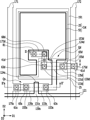
1. A transistor display panel comprising:
a substrate;
a lower electrode disposed on the substrate;
a buffer layer covering the lower electrode;
a transistor disposed on the substrate; and
a pixel electrode connected to the transistor,
wherein the transistor includes:
a semiconductor on the substrate,
a first insulating layer disposed on the semiconductor,
a gate electrode on the first insulating layer overlapping the semiconductor,
a second insulating layer covering the gate electrode, and
a source electrode and a drain electrode disposed on the second insulating layer,
wherein the lower electrode is disposed under the semiconductor and is electrically connected to the pixel electrode,
wherein the semiconductor includes a channel, and a source region and a drain region disposed at respective sides of the channel, and
wherein the source region and the drain region are respectively connected to the source electrode and the drain electrode.
|