| CPC H10K 59/12 (2023.02) [H10K 50/844 (2023.02); H10K 71/00 (2023.02); H10K 77/111 (2023.02); H10K 59/1201 (2023.02)] | 15 Claims |
|
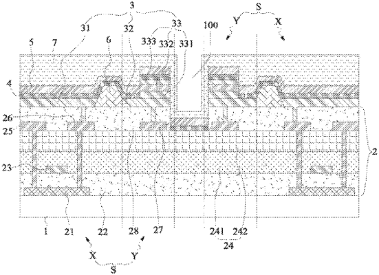
1. A flexible display panel, comprising:
a flexible substrate and a plurality of pixel islands arranged in an array on the flexible substrate, wherein the pixel island has a display area and a peripheral area surrounding the display area, and each of the pixel islands comprises a driving layer, a first electrode layer, a light emitting layer, and a second electrode layer sequentially laminated on the flexible substrate,
wherein the first electrode layer comprises a first electrode located in the display area and a peripheral electrode located in the peripheral area, the peripheral electrode surrounds the display area, and a surface of the peripheral electrode away from the flexible substrate is provided with a blocking structure surrounding the display area, a preset interval exists between the blocking structure and the display area; and an area of the light emitting layer located in a range of the blocking structure and an area of the light emitting layer located in a range of the preset interval are interruptedly arranged.
|