| CPC H10K 50/844 (2023.02) [H10K 50/8426 (2023.02); H10K 59/131 (2023.02); H10K 59/88 (2023.02); H10K 71/00 (2023.02); H10K 77/111 (2023.02); H10K 59/1201 (2023.02); H10K 71/851 (2023.02); H10K 2102/00 (2023.02); H10K 2102/311 (2023.02); Y02E 10/549 (2013.01)] | 15 Claims |
|
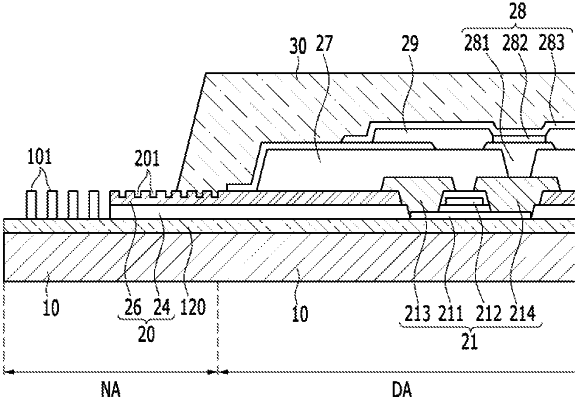
1. A display device, comprising:
a substrate;
a display area and a non-display area on the substrate;
a barrier layer disposed on the substrate;
a thin film transistor disposed on the barrier layer in the display area and including an active layer, a first electrode, a second electrode, and a third electrode;
a first insulating layer disposed between the active layer and the first electrode;
a second insulating layer disposed between the first electrode and the third electrode;
a first pattern disposed in the non-display area and is formed of a same metal material as one of the first electrode, the second electrode, and the third electrode;
a plurality of second patterns disposed in the non-display area and is formed of a same insulating material as one of the first insulating layer and the second insulating layer; and
a third pattern disposed in the non-display area,
wherein the plurality of second patterns are disposed between the first pattern and the third pattern;
and wherein the first pattern and the plurality of second patterns do not overlap in a direction perpendicular to a surface of the substrate.
|