| CPC H10K 50/844 (2023.02) [H10K 59/1201 (2023.02); H10K 59/131 (2023.02)] | 16 Claims |
|
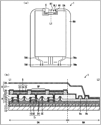
1. A display device comprising:
a display region;
a frame region surrounding the display region; and
a cutout portion provided in the frame region,
wherein a resin layer, a plurality of inorganic insulating films formed on the resin layer, and a metal layer formed on and in contact with one inorganic insulating film from among the plurality of inorganic insulating films are provided,
a metal pattern formed from the metal layer is formed, conforming to at least a portion of a shape of the cutout portion in the frame region between a variant edge portion of the display device forming the cutout portion and the display region, the display region being provided with a plurality of subpixels, and
the metal pattern is electrically unconnected to any wiring lines.
|