| CPC H10K 50/805 (2023.02) [H10K 50/8445 (2023.02); H10K 59/122 (2023.02); H10K 2102/101 (2023.02)] | 10 Claims |
|
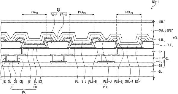
1. A method for manufacturing a display device, the method comprising:
providing a preliminary display device comprising a circuit element layer on which a transistor is formed, a first electrode connected to the transistor, a pixel defining layer in which an opening exposing the first electrode is formed, and an auxiliary electrode covering a portion of the pixel defining layer;
forming a lift-off layer covering the preliminary display device;
forming a photoresist layer covering the lift-off layer;
removing areas of the lift-off layer and the photoresist layer, which overlap the opening, to form an under cut;
forming an organic pattern overlapping the opening, a second electrode covering the organic pattern and connected to the auxiliary electrode, a first protection pattern covering the second electrode, and a second protection pattern covering the first protection pattern; and
removing the lift-off layer and the photoresist layer,
wherein the first protection pattern and the second protection pattern have stress in directions different from each other.
|