| CPC H10K 30/88 (2023.02) [H10K 30/20 (2023.02); H10K 77/10 (2023.02); H10K 85/113 (2023.02); H10K 85/211 (2023.02); H10K 85/30 (2023.02)] | 14 Claims |
|
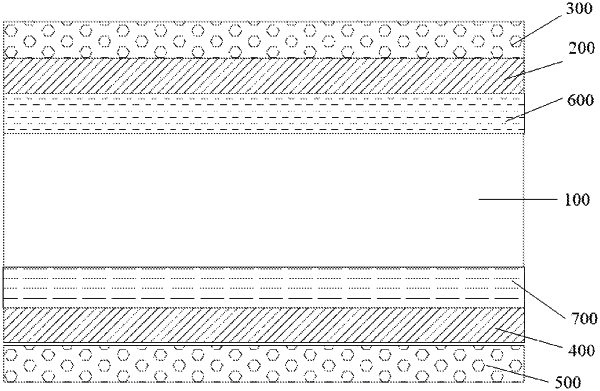
1. A solar cell, comprising:
a semiconductor substrate having a first surface and a second surface opposite to the first surface;
a first passivation layer and a first electrode layer that are located on the first surface of the semiconductor substrate; and
a second passivation layer and a second electrode layer that are located on the second surface of the semiconductor substrate,
wherein a donor material film layer is provided between the first passivation layer and the first surface of the semiconductor substrate, and an acceptor material film layer is provided between the second passivation layer and the second surface of the semiconductor substrate,
wherein an acceptor material of the acceptor material film layer has an electron mobility of 1 cm2V−1S−1 to 50 cm2V−1S−1, a lowest unoccupied molecular orbital (LUMO) energy level of −2.8 eV to −3.6 eV, a highest occupied molecular orbital (HOMO) energy level of −5.2 eV to −5.6 eV, and an optical band gap of 1.7 eV to 4 eV,
wherein a donor material of the donor material film layer has a hole mobility of 1×10⁻⁶ cm2V−1S−1 to 1×10⁻² cm2V−1S−1, a LUMO energy level of −3.2 eV to −3.6 eV, a HOMO energy level of −5.2 eV to −6.4 eV, and an optical band gap of 1.7 eV to 4 eV,
wherein the acceptor material film layer comprises an organic acceptor material having electron transport capability, and the organic acceptor material comprises at least one of a fullerene-based acceptor material and a non-fullerene-based acceptor material, and
wherein the donor material film layer comprises at least one of a polythiophene material having hole transport capability, a fluorene-containing polymer material, a small-molecule photovoltaic material containing a benzodithiophene electron donor element and a small-molecule photovoltaic material containing a porphyrin unit.
|