| CPC H10B 69/00 (2023.02) [G11C 7/16 (2013.01); G11C 8/14 (2013.01); G11C 11/24 (2013.01); G11C 11/403 (2013.01); G11C 11/4085 (2013.01); H01L 27/0688 (2013.01); H01L 29/24 (2013.01); H01L 29/7869 (2013.01); H10B 41/20 (2023.02); H10B 41/70 (2023.02)] | 11 Claims |
|
1. A semiconductor device comprising:
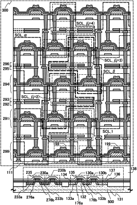
a memory cell including first to cth sub memory cells (c is a natural number greater than or equal to 2),
wherein a jth sub memory cell includes a first transistor, a capacitor, and a second transistor (j is a natural number of 1 to c),
wherein a first semiconductor layer in the first transistor and a second semiconductor layer in the second transistor include an oxide semiconductor,
wherein one of terminals of the capacitor is electrically connected to a gate of the second transistor through a plug,
wherein the one of the terminals of the capacitor is electrically connected to one of a source electrode and a drain electrode of the first transistor through a plug,
wherein, when j≥2, the jth sub memory cell is arranged over a j-lth sub memory cell,
wherein a bit line is electrically connected to an other of the source electrode and the drain electrode of the first transistor of the jth sub memory cell, and
wherein the bit line is electrically connected to one of a source electrode and a drain electrode of the first transistor of the j-lth sub memory cell.
|