| CPC H10B 63/30 (2023.02) [H01L 29/66795 (2013.01); H01L 29/785 (2013.01); H10N 70/021 (2023.02); H10N 70/826 (2023.02); H10N 70/882 (2023.02); H10N 70/8833 (2023.02)] | 25 Claims |
|
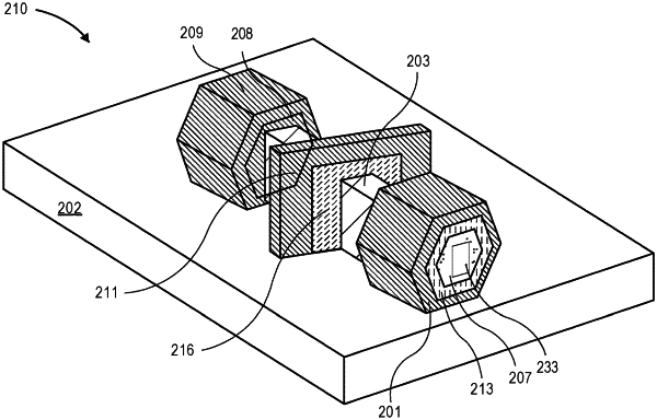
1. A semiconductor device, comprising:
a FinFET transistor including a fin structure on a substrate, wherein the fin structure includes a channel region, a source region adjacent to the channel region, and a drain region adjacent to the channel region, an epitaxial layer around the source region or the drain region; and
a resistive random access memory (RRAM) storage stack wrapped around a surface of the epitaxial layer, the RRAM storage stack including:
a resistive switching material layer in contact and wrapped around the surface of the epitaxial layer; and
a contact electrode in contact and wrapped around a surface of the resistive switching material layer, wherein the epitaxial layer, the resistive switching material layer, and the contact electrode form a RRAM storage cell.
|