| CPC H10B 51/30 (2023.02) [H01L 29/40111 (2019.08); H01L 29/516 (2013.01); H01L 29/6684 (2013.01); H01L 29/78391 (2014.09); H10B 51/40 (2023.02)] | 20 Claims |

|
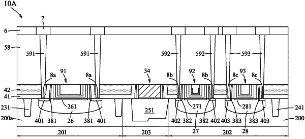
1. A method for manufacturing an integrated circuit, comprising:
forming a boundary isolation in a semiconductor substrate;
forming a memory well and a logic well in the semiconductor substrate, the memory well and the logic well being located at two opposite sides of the boundary isolation, the memory well having two memory source/drain regions and a memory channel region between the two memory source/drain regions, the logic well having two logic source/drain regions and a logic channel region between the two logic source/drain regions;
forming a dummy wall on the boundary isolation, the dummy wall including a dummy gate portion and a dummy dielectric portion, and having a rectangular cross section;
forming a patterned dielectric structure on the semiconductor substrate to expose the dummy wall, the patterned dielectric structure having a first recess which exposes the memory channel region, and a second recess which exposes the logic channel region;
forming a data storage element along a surface of the first recess;
forming a gate dielectric along a surface of the second recess;
forming a memory gate in the first recess such that the data storage element is disposed around the memory gate; and
forming a logic gate in the second recess such that the gate dielectric is disposed around the logic gate,
wherein the semiconductor substrate includes a memory substrate region, a logic substrate region, and a boundary substrate region between the memory substrate region and the logic substrate region, the boundary isolation being formed in the boundary substrate region, the memory well and the logic well being formed in the memory substrate region and the logic substrate region, respectively;
wherein the formation of the data storage element includes:
conformally depositing a ferroelectric layer over the patterned dielectric structure along the surface of the first recess and along the surface of the second recess,
partially removing the ferroelectric layer such that a first ferroelectric portion of the ferroelectric layer is left on the memory substrate region, and
removing an excess of the first ferroelectric portion such that a region of the first ferroelectric portion is left on the surface of the first recess to serve as the data storage element and
wherein the formation of the gate dielectric includes:
conformally depositing a gate dielectric layer over the patterned dielectric structure, on the first ferroelectric portion, and along the surface of the second recess, and
removing an excess of the gate dielectric layer such that a portion of the gate dielectric layer is left on the surface of the second recess to serve as the gate dielectric.
|