| CPC H10B 43/35 (2023.02) [G11C 16/14 (2013.01); H01L 29/0649 (2013.01); H01L 29/42328 (2013.01); H01L 29/42344 (2013.01); H01L 29/7851 (2013.01); H10B 41/10 (2023.02); H10B 41/35 (2023.02); H10B 43/10 (2023.02)] | 19 Claims |
|
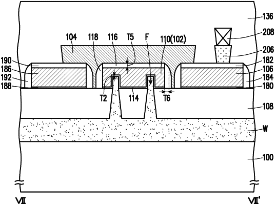
1. A memory structure, comprising:
a substrate having a fin portion;
a gate structure, wherein a portion of the gate structure is disposed on the fin portion, and the gate structure and the fin portion are electrically insulated from each other;
a charge storage layer coupled to the gate structure, wherein the charge storage layer and the gate structure are electrically insulated from each other; and
a first control gate coupled to the charge storage layer, wherein the first control gate and the charge storage layer are electrically insulated from each other,
wherein the gate structure comprises:
a first gate disposed on the fin portion, wherein the first gate and the fin portion are electrically insulated from each other; and
a second gate, not disposed on the fin portion, and wherein the first gate and the second gate are separated from each other and electrically connected to each other, the charge storage layer is coupled to the second gate, and the charge storage layer and the second gate are electrically insulated from each other.
|