| CPC H10B 43/27 (2023.02) [H01L 21/76816 (2013.01); H01L 21/76877 (2013.01); H01L 23/5226 (2013.01); H01L 23/5283 (2013.01); H01L 23/53257 (2013.01); H01L 23/53271 (2013.01); H10B 41/27 (2023.02); H10B 41/35 (2023.02); H10B 43/35 (2023.02)] | 17 Claims |
|
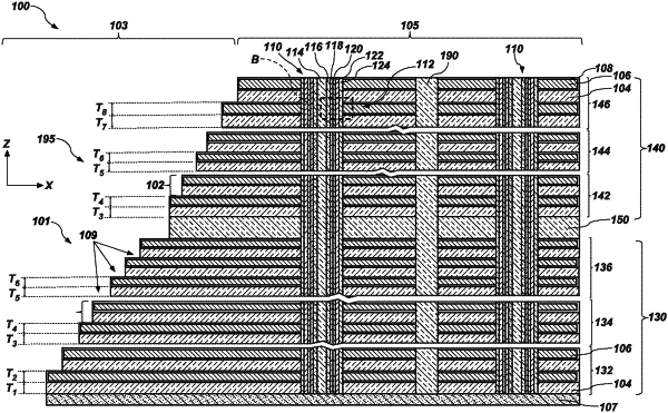
1. A microelectronic device, comprising:
a stack structure comprising tiers each comprising a level of conductive material and a level of insulative material vertically neighboring the level of conductive material, a vertical thickness of a lowermost one of the tiers larger than a vertical thickness of an uppermost one of the tiers, a vertical thickness of the insulative material of the lowermost one of the tiers greater than a vertical thickness of the insulative material of the uppermost one of the tiers; and
strings of memory cells vertically extending through the stack structure.
|