| CPC H10B 43/27 (2023.02) [H01L 21/28525 (2013.01); H01L 21/76805 (2013.01); H01L 21/76823 (2013.01); H01L 21/76834 (2013.01); H01L 21/76895 (2013.01); H01L 23/535 (2013.01); H01L 23/53271 (2013.01); H10B 41/27 (2023.02)] | 13 Claims |
|
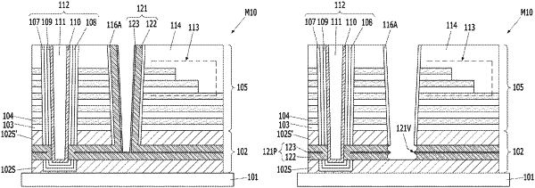
1. A method for fabricating a vertical semiconductor device, comprising:
forming a first multi-layer stack in which a source sacrificial layer is positioned over a lower source layer, the lower source layer over a lower structure;
forming a second multi-layer stack in which dielectric layers and sacrificial layers are alternately stacked over the first multi-layer stack;
forming a vertical structure that penetrates the second multi-layer stack and the first multi-layer stack, and includes a channel layer insulated from the lower source layer;
forming a vertical contact recess that penetrates the second multi-layer stack and the first multi-layer stack and exposes the source sacrificial layer;
forming a horizontal contact recess extending from the vertical contact recess by removing the source sacrificial layer;
exposing a side of the channel layer of the vertical structure by extending the horizontal contact recess;
forming a source channel contact that fills the horizontal contact recess, and includes a first conductive layer in contact with the channel layer and a second conductive layer doped with a dopant which is different from a dopant of the first conductive layer, and
forming a barrier oxide formed on the first and second conductive layers,
wherein the source channel contact includes a concave portion and a convex portion, the concave portion and the convex portion are directly contacted with the barrier oxide,
wherein the convex portion of the source channel contact has a peak, and the peak is provided by the second conductive layer, and
wherein the concave portion and the convex portion of the source channel contact are fully covered by the barrier oxide.
|