| CPC H10B 43/27 (2023.02) [H01L 21/0273 (2013.01); H01L 21/02164 (2013.01); H01L 21/02532 (2013.01); H01L 21/02579 (2013.01); H01L 21/02595 (2013.01); H01L 21/02636 (2013.01); H01L 21/30604 (2013.01); H01L 21/31053 (2013.01); H01L 21/31111 (2013.01); H01L 21/31144 (2013.01); H01L 21/76802 (2013.01); H01L 21/76877 (2013.01); H01L 29/0847 (2013.01)] | 21 Claims |
|
1. A process for forming a memory structure over a planar surface of a semiconductor substrate, comprising:
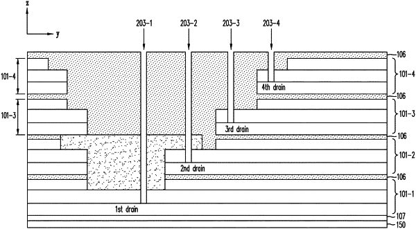
forming above the semiconductor substrate a plurality of active stacks placed substantially at predetermined positions along a first direction that is substantially parallel to the planar surface, separated one from another by a first electrically insulative material, each active stack extending lengthwise along a second direction that is (i) substantially parallel to the planar surface and (ii) substantially orthogonal the first direction, wherein (i) each active stack comprises a plurality of active strips, provided along at predetermined positions along a third direction that is substantially orthogonal to the planar surface, each active strip being separated one from another by a first isolation layer; and (ii) each active strip comprises (a) first and second semiconductor layers of a first conductivity type, and (b) a second isolation layer separating the first and the second semiconductor layers;
patterning and etching the first electrically insulative material to provide a plurality of openings at predetermined positions along the first direction, the openings each extending along the third direction, exposing sidewalls of the active stacks on opposite sides of the opening;
etching the second isolation layer of each active strip through the openings, thereby creating recesses between the first and the second semiconductor layers at opposite sides of the second isolation layer;
conformally depositing a third semiconductor layer, the third semiconductor layer being of a second conductivity opposite the first conductivity, such that the third semiconductor layer lines the sidewalls of the opening and one or more walls of the recesses of each active strip;
anisotropically etching the third semiconductor layer to remove the third semiconductor layer from the sidewalls of the openings;
conformally depositing a charge-trapping material on the sidewalls of the opening, such that the third semiconductor layer in the recesses are in contact with the charge-trapping layer; and
filling the openings with a conductive material.
|