| CPC H10B 43/27 (2023.02) [H10B 41/10 (2023.02); H10B 41/27 (2023.02); H10B 41/30 (2023.02); H10B 41/40 (2023.02); H10B 43/10 (2023.02); H10B 43/30 (2023.02); H10B 43/40 (2023.02)] | 16 Claims |
|
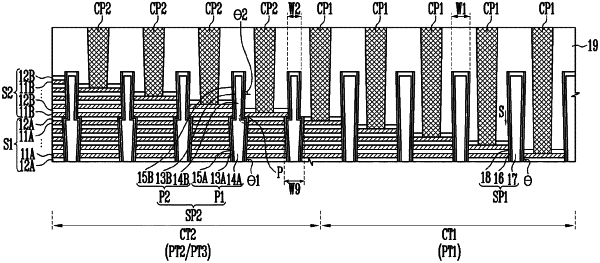
1. A method of manufacturing a semiconductor device, the method comprising:
forming a first patterned stack structure including a cell region, a first portion in a first contact region, and a second portion in a second contact region, the second portion of the first patterned stack structure including a first opening;
forming a second patterned stack structure including a third portion over the cell region and the second contact region of the first patterned stack structure;
forming a second opening penetrating the third portion of the second patterned stack structure, the second opening being coupled to the first opening; and
forming a third opening penetrating the first portion of the first patterned stack structure when the second opening is formed,
wherein a diameter of a top of the third opening is greater than a diameter of a top of the second opening.
|