| CPC H10B 43/20 (2023.02) [G11C 7/18 (2013.01); G11C 16/0466 (2013.01); G11C 16/08 (2013.01); G11C 16/24 (2013.01); H03K 19/1776 (2013.01); H03K 19/20 (2013.01); H01L 29/78696 (2013.01)] | 12 Claims |
|
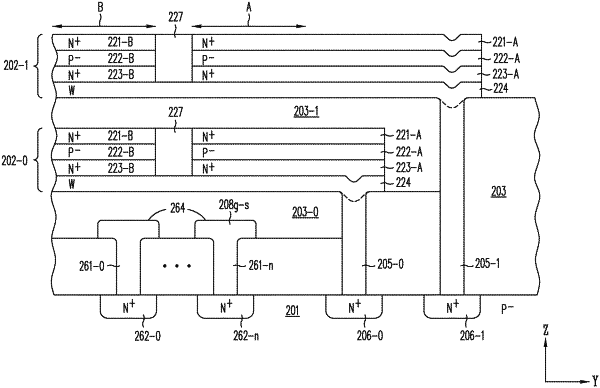
1. An array of NOR memory strings, formed above a planar surface of a semiconductor substrate, the memory array comprising:
a channel layer extending lengthwise along a first direction that substantially parallels the planar surface;
a source layer and a drain layer each being in contact with the channel layer but separated from each other, the source layer and the drain layer each extending lengthwise along the first direction, wherein (i) the source layer comprises a first segment and a second segment that are electrically isolated from each other, (ii) a first portion of the channel layer, the first segment of the source layer and the drain layer form storage transistors of a first one of the NOR memory strings, and a second portion of the channel layer, the second segment of the source layer and the drain layer form storage transistors of a second one of the NOR memory strings; and (iii) as to storage transistors in each NOR memory string, the drain layer provides a common bit line, and the corresponding segment of the source layer provides a common source line;
a layer of storage material provided in a trench that runs lengthwise along the first direction through the drain layer, the source layer and the channel layer; and
a plurality of conductors to serve as local word lines.
|