| CPC H10B 41/27 (2023.02) [G11C 5/025 (2013.01); G11C 16/08 (2013.01); G11C 16/26 (2013.01); H01L 25/0657 (2013.01); H10B 43/27 (2023.02)] | 14 Claims |
|
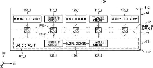
1. A semiconductor device comprising:
a first chip configured to include a peripheral circuit; and
a second chip stacked on the first chip, and configured to include a first memory cell array and a second memory cell array,
wherein a plurality of transfer circuits configured to connect a plurality of row lines of the first memory cell array and a plurality of row lines of the second memory cell array to respective global row lines is divided between the first chip and the second chip
wherein the first chip includes:
a first transfer circuit configured to connect a global row line to a row line of the first memory cell array in response to a row line selection signal;
a second transfer circuit configured to connect the global row line to a row line of the second memory cell array in response to the row line selection signal; and
a global decoder configured to provide an operation voltage to each of the first transfer circuit, the second transfer circuit, and a transfer circuit disposed in the second chip through the global row line.
|