| CPC H10B 41/27 (2023.02) [G11C 5/025 (2013.01); H01L 23/528 (2013.01); H10B 43/27 (2023.02)] | 16 Claims |
|
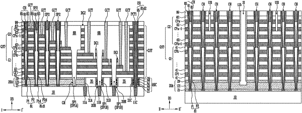
1. A semiconductor memory device, comprising:
a first stack including lower conductive patterns separated from each other and stacked over a substrate to form a lower stepped structure;
a second stack including upper conductive patterns separated from each other and stacked over the first stack to form an upper stepped structure, wherein the second stack does not overlap with the lower stepped structure;
an insulating layer covering the lower stepped structure and the upper stepped structure;
a first support pillar extending from the insulating layer to pass through the first stack;
a channel structure passing through the second stack and the first stack;
a memory layer adjacent to a sidewall of the channel structure; and
a channel connecting pattern arranged between the substrate and the first stack, the channel connecting pattern penetrating the memory layer to contact the channel structure,
wherein the channel connecting pattern extends into a groove included in the first support pillar.
|