| CPC H10B 12/488 (2023.02) [G11C 5/063 (2013.01); H01L 24/08 (2013.01); H01L 24/80 (2013.01); H10B 12/482 (2023.02); H01L 2224/08145 (2013.01); H01L 2224/80896 (2013.01); H01L 2924/1431 (2013.01); H01L 2924/1436 (2013.01)] | 34 Claims |
|
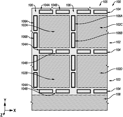
16. A method of forming a microelectronic device, comprising:
forming a first semiconductor wafer comprising memory cells within array regions, digit lines coupled to the memory cells and terminating within digit line exit regions neighboring the array regions, and word lines coupled to the memory cells and terminating within word line exit regions neighboring the array regions;
forming digit line contacts within the digit line exit regions, the digit line contacts coupled to the digit lines and horizontally surrounded by air gaps;
forming word line contacts within the word line exit regions, the word line contacts coupled to the word lines and horizontally surrounded by additional air gaps;
forming a second semiconductor wafer comprising control logic devices;
attaching the second semiconductor wafer to the first semiconductor wafer through oxide-oxide bonding;
coupling the digit line contacts to some of the control logic devices; and
coupling the word line contacts to some other of the control logic devices.
|