| CPC H10B 12/482 (2023.02) [H01L 21/67167 (2013.01); H01L 21/67213 (2013.01)] | 16 Claims |
|
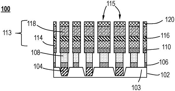
1. A non-transitory computer readable medium including instructions, that, when executed by a controller of a processing chamber, cause the processing chamber to perform operations of forming a dynamic random access memory (DRAM) bit line, comprising:
implant an inert species into a bit line metal layer having a first grain size on a substrate to form an amorphized bit line metal layer having a second grain size smaller than the first grain size;
deposit a film stack on the amorphized bit line metal layer;
etch the film stack and the amorphized bit line metal layer to form a patterned film stack on the substrate, the patterned film stack comprising a plurality of the DRAM bit line; and
thermally anneal the patterned film stack on the substrate at a temperature in a range of about 500° C. to about 900° C. to increase the second grain size of the amorphized bit line metal layer to a third grain size larger than the second grain size.
|