| CPC H10B 12/315 (2023.02) [H10B 12/0335 (2023.02); H10B 12/34 (2023.02); H10B 12/482 (2023.02)] | 8 Claims |
|
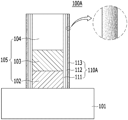
1. A semiconductor device, comprising:
a bit line structure formed over a substrate;
a storage node contact plug spaced apart from the bit line structure; and
a nitride spacer positioned between the bit line structure and the storage node contact plug,
wherein the nitride spacer has a higher silicon content in a portion adjacent to the storage node contact plug than in a portion adjacent to the bit line structure.
|