| CPC H10B 12/30 (2023.02) [G11C 11/4097 (2013.01)] | 20 Claims |
|
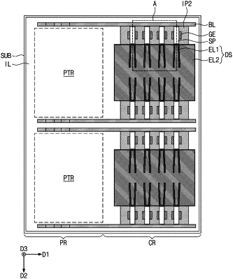
1. A semiconductor device comprising:
a substrate;
a semiconductor pattern on the substrate, and extending in a first direction that is parallel to a top surface of the substrate, the semiconductor pattern including a first region, a second region, and a third region between the first region and the second region;
a word line arranged adjacent to the third region of the semiconductor pattern, and extending in a second direction that is perpendicular to the top surface of the substrate;
a bit line contacting the first region of the semiconductor pattern, and extending in a third direction that is parallel to the top surface of the substrate and that is perpendicular to the first direction; and
a lower electrode contacting the second region of the semiconductor pattern, and extending in the first direction, the lower electrode including a first portion that is adjacent to the second region of the semiconductor pattern, and a second portion that is on the first portion;
a dielectric layer on the lower electrode; and
an upper electrode on the dielectric layer,
wherein a width of the first portion of the lower electrode in the third direction is less than a width of the second portion of the lower electrode in the third direction, and
a width of the first portion of the lower electrode in the second direction is substantially equal to a width of the second portion of the lower electrode in the second direction.
|