| CPC H10B 12/30 (2023.02) [H01L 29/0847 (2013.01); H10B 12/03 (2023.02); H10B 12/05 (2023.02)] | 20 Claims |
|
1. A semiconductor memory device comprising:
a bit line on a substrate, the bit line extending in a vertical direction;
a transistor body comprising a first source-drain region, a monocrystalline channel layer, and a second source-drain region, the first source-drain region, the monocrystalline channel layer, and the second source-drain region sequentially arranged in a first horizontal direction, the transistor body connected to the bit line;
gate electrode layers extending in a second horizontal direction orthogonal to the first horizontal direction; with a gate dielectric layer between the gate electrode layers and a portion of the transistor body, the gate dielectric layer covering upper surfaces and lower surfaces of the monocrystalline channel layer; and
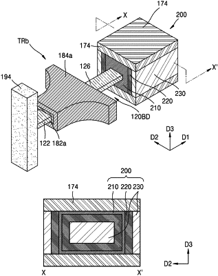
a cell capacitor at a side of the transistor body that is opposite to the bit line in the first horizontal direction, the cell capacitor connected to the second source-drain region, the cell capacitor comprising a first electrode layer, a capacitor dielectric layer, and second electrode layers,
the first electrode layer, the dielectric layer, and the second electrode layers extending in the first horizontal direction, the dielectric layer spaced between the first electrode layer and the second electrode layers in the second horizontal direction, the first electrode layer and the second electrode layers configured to generate an electric field extending in the first horizontal direction and the vertical direction.
|