| CPC H10B 12/00 (2023.02) [H01L 21/28556 (2013.01); H01L 21/31053 (2013.01); H01L 21/31144 (2013.01); H01L 21/67069 (2013.01); H01L 21/67075 (2013.01); H01L 21/76829 (2013.01); H10B 99/00 (2023.02)] | 8 Claims |
|
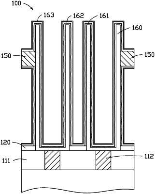
1. A method for fabricating a semiconductor device, the method comprising:
providing a substrate having an etch stop layer formed thereon;
forming a preliminary stacked structure on the etch stop layer, the preliminary stacked structure including a lower sacrifice layer contacting the etch stop layer, a support layer, and an upper sacrifice layer;
forming a hole penetrating the preliminary stacked structure and the etch stop layer;
forming a conductive pattern in the hole;
removing the upper sacrifice layer and a portion of the support layer;
removing the lower sacrifice layer;
forming a first conductive layer covering the conductive pattern; and
forming a dielectric layer covering the first conductive layer, a remaining portion of the support layer, and the etch stop layer.
|