| CPC H10B 10/18 (2023.02) | 8 Claims |
|
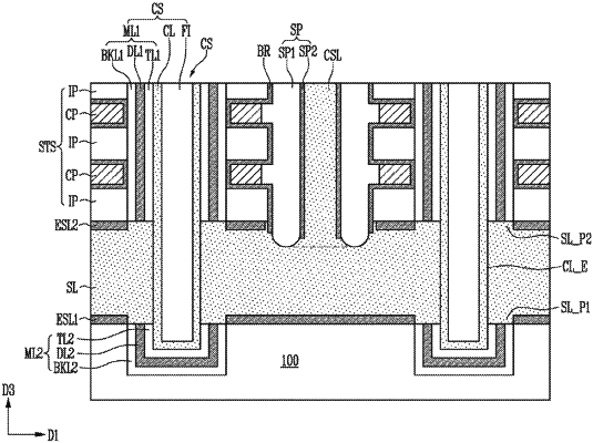
1. A method of manufacturing a semiconductor memory device, the method comprising:
forming a base part;
sequentially forming, on the base part, a first etch stop layer, a source sacrificial layer, and a second etch stop layer;
forming a stack structure, including insulating patterns, on the second etch stop layer;
forming a channel structure that penetrates the stack structure, the second etch stop layer, the source sacrificial layer, and the first etch stop layer, wherein a portion of the channel structure is disposed in a portion of the base part;
forming a first trench that penetrates the stack structure and the second etch stop layer;
removing the source sacrificial layer; and
forming a source layer between the first and second etch stop layers.
|