| CPC H05K 9/0079 (2013.01) [C08G 61/126 (2013.01); C08G 73/0611 (2013.01); C08G 85/004 (2013.01); H01L 21/4867 (2013.01); H01L 23/60 (2013.01); C08G 2261/1424 (2013.01); C08G 2261/3223 (2013.01); C08G 2261/514 (2013.01); C08G 2261/78 (2013.01); H01L 23/498 (2013.01)] | 20 Claims |
|
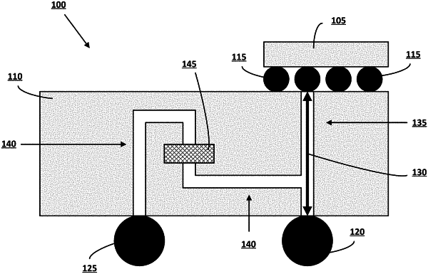
1. A microelectronic package comprising:
a die; and
a package substrate coupled to the die with a first interconnect on a first face, wherein the package substrate comprises:
a second interconnect and a third interconnect on a second face opposite to the first face;
a conductive signal path between the first interconnect and the second interconnect;
a conductive ground path between the second interconnect and the third interconnect; and
an electrostatic discharge (ESD) protection material coupled to the conductive ground path, the ESD protection material comprising a first electrically-conductive carbon allotrope having a first functional group, a second electrically-conductive carbon allotrope having a second functional group, and an electrically-conductive polymer that is chemically bonded to the first functional group and the second functional group permitting an electrical signal to pass between the first and second electrically-conductive carbon allotropes.
|