| CPC H05K 5/0269 (2013.01) [G06F 1/182 (2013.01); G06F 3/0688 (2013.01); H05K 7/20472 (2013.01); H05K 1/0275 (2013.01); H05K 1/144 (2013.01); H05K 7/20454 (2013.01); H05K 2201/042 (2013.01); H05K 2201/10159 (2013.01)] | 20 Claims |
|
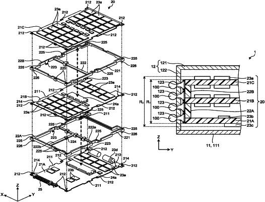
1. A solid state drive comprising:
a first printed circuit board having a first main surface and a second main surface, the second main surface opposing the first main surface;
a flash memory;
a first encryption device mounted on the first main surface, the first encryption device being configured to encrypt data to be stored in the flash memory; and
a housing including a wall and a first plate, the housing accommodating the first printed circuit board, the flash memory, and the first encryption device,
the wall including a first region and a second region, the first region including an opening, the second region including no opening,
the first plate having a first surface, the first surface facing the first main surface of the first printed circuit board,
wherein
the second region of the wall is bounded by a first position and a second position,
the first position being a position where the wall is intersected by an imaginary extension of the first main surface of the first printed circuit board,
the second position being a position where the wall is intersected by an imaginary extension of the first surface of the first plate.
|