| CPC H05K 3/46 (2013.01) [H05K 1/0298 (2013.01); H05K 3/10 (2013.01); H05K 2203/0502 (2013.01); Y10T 29/49147 (2015.01)] | 4 Claims |
|
1. A method of producing a wiring board that comprises a board, a conductor pattern on the board, and an insulating film covering at least part of the conductor pattern, the method comprising:
transferring first ink of insulating film material from a first flexographic plate onto the board so that the first ink of insulating film material is provided in a first region covering said at least part of the conductor pattern on the board, the first region having a first border segment;
curing the first ink of insulating film material provided in the first region;
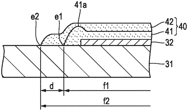
transferring second ink of insulating film material from a second flexographic plate onto the board so that the second ink of insulating film material is provided in a second region covering at least part of the first region on the board, the second region having a second border segment that is located beyond the first region, wherein a shortest distance between the first border segment and any point belonging to the second border segment is not less than 50 μm and not greater than 400 μm; and
curing the second ink of insulating film material provided in the second region, whereby the insulating film is gained as a combination of cured products of the first ink of insulating film material and the second ink of insulating film material.
|