| CPC H05K 1/185 (2013.01) [H05K 1/112 (2013.01); H05K 1/183 (2013.01); H05K 2201/096 (2013.01)] | 18 Claims |
|
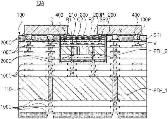
1. A printed circuit board comprising:
a first substrate including a first cavity and first circuit units; and
a second substrate disposed in the first cavity of the first substrate with an electronic component disposed therein, and including second circuit units having a higher density than the first circuit units,
wherein the second substrate includes a first region and a second region,
the first region of the second substrate includes an outermost circuit layer among the second circuit units,
circuit layers in the first region of the second substrate have a higher density than circuit layers in the second region of the second substrate, and
along a stacking direction of the circuit layers, the second circuit units overlap the electronic component.
|