| CPC H05K 1/144 (2013.01) [H05K 1/028 (2013.01); H05K 1/115 (2013.01); H05K 1/118 (2013.01); H05K 3/363 (2013.01); H05K 2201/041 (2013.01); H05K 2201/0939 (2013.01); H05K 2201/09481 (2013.01)] | 17 Claims |
|
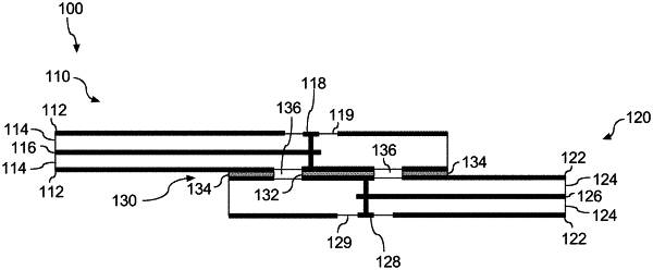
1. An interconnection for connecting a plurality of flex circuit boards, comprising:
a first flex circuit board having a first side and a second side opposite the first side;
a second flex circuit board having a third side and a fourth side opposite the third side;
wherein the first flex circuit board and the second flex circuit board are physically coupled to each other in an overlap joint in which a portion of the second side of the first flex circuit board overlaps a portion of the third side of the flex circuit board;
wherein the first flex circuit board comprises:
a first signal line;
a first dielectric layer; and
a first via extending through the first dielectric layer at least from the first signal line to the second side of the first flex circuit board;
wherein the second flex circuit board comprises:
a second signal line;
a second dielectric layer; and
a second via extending through the second dielectric layer at least from the second signal line to the third side of the second flex circuit board; and
wherein the interconnection further comprises a signal pad structure positioned in the overlap joint between the second side of the first flex circuit board and the third side of the second flex circuit board and electrically coupled to the first via and the second via
wherein the first via and the second via are offset in the overlap joint;
wherein the first signal line and the second signal line comprise a superconducting material that achieves superconductivity at a temperature of less than about 3 Kelvin.
|