| CPC H05K 1/028 (2013.01) [H05K 1/0296 (2013.01); H05K 3/02 (2013.01); H05K 2201/055 (2013.01)] | 20 Claims |

|
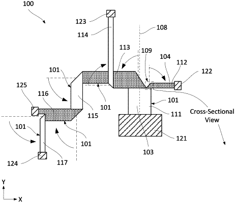
1. A method of forming a flexible interconnect circuit assembly, the method comprising:
providing a flexible interconnect circuit comprising a first circuit portion and a second circuit portion monolithically integrated with the first circuit portion, wherein:
each of the first circuit portion and the second circuit portion is an elongated structure extending parallel to a primary axis of the flexible interconnect circuit,
each of the first circuit portion and the second circuit portion comprises a first side and a second side opposite to the first side, and
the first side of the first circuit portion and the first side of the second circuit portion face in a same direction;
folding the second circuit portion relative to the first circuit portion such that the second circuit portion is no longer parallel to the primary axis of the flexible interconnect circuit and such that the second side of the first circuit portion and the second side of the second circuit portion face in opposite directions after folding;
attaching a bonding film to the second side of the first circuit portion and the first side of the second circuit portion; and
attaching a temporary support film to the bonding film such that the first side of the first circuit portion and the second side of the second circuit portion face the temporary support film.
|