US 11,751,322 B2
Integrating graphene into the skin depth region of high speed communications signals for a printed circuit board
Joel Goergen, Soulsbyville, CA (US); Scott Hinaga, Palo Alto, CA (US); Jessica Kiefer, San Jose, CA (US); Alpesh Umakant Bhobe, Sunnyvale, CA (US); D. Brice Achkir, Livermore, CA (US); David Nozadze, San Jose, CA (US); Amendra Koul, San Francisco, CA (US); Mehmet Onder Cap, Sunnyvale, CA (US); and Madeline Marie Roemer, Los Altos, CA (US)
Assigned to CISCO TECHNOLOGY, INC., San Jose, CA (US)
Filed by Cisco Technology, Inc., San Jose, CA (US)
Filed on Mar. 24, 2022, as Appl. No. 17/703,051.
Application 17/703,051 is a continuation of application No. 17/079,970, filed on Oct. 26, 2020, granted, now 11,330,702.
Claims priority of provisional application 63/016,500, filed on Apr. 28, 2020.
Prior Publication US 2022/0217837 A1, Jul. 7, 2022
This patent is subject to a terminal disclaimer.
Int. Cl. H05K 1/02 (2006.01)
CPC H05K 1/0239 (2013.01) [H05K 1/0242 (2013.01); H05K 2201/09245 (2013.01)] 20 Claims
OG exemplary drawing
 
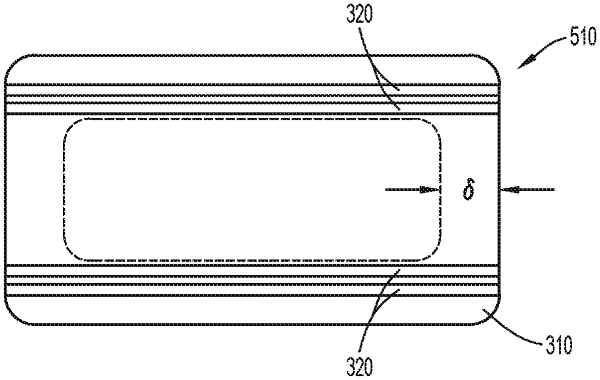
1. A conductive signal transmission structure for transmission of signals for an electronic device, the conductive signal transmission structure comprising a copper material and a plurality of graphene layers, each graphene layer being disposed within the copper material at a depth below a corresponding surface of the conductive signal transmission structure, wherein the depth of each graphene layer below the corresponding surface of the conductive signal transmission structure is within a skin depth region of the conductive signal transmission structure when a transmission signal applied to the conductive signal transmission structure has a signal speed of at least 112 Gbps.