| CPC H04W 56/001 (2013.01) [H04L 5/0048 (2013.01)] | 30 Claims |
|
1. A user equipment (UE) for wireless communication, comprising:
a memory; and
one or more processors coupled to the memory, the one or more processors configured to:
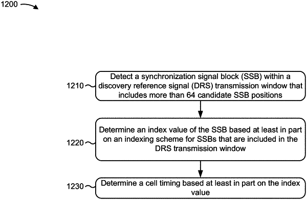
detect a synchronization signal block (SSB) within a discovery reference signal (DRS) transmission window that includes more than 64 candidate SSB positions;
determine an index value of the SSB based at least in part on an indexing scheme for SSBs that are included in the DRS transmission window, wherein the indexing scheme comprises:
a non-consecutive indexing scheme in which a first subset of the SSBs are indexed in ascending order from earlier positions in the DRS transmission window to later positions in the DRS transmission window and a second subset of the SSBs are indexed in ascending order from earlier positions in the DRS transmission window to later positions in the DRS transmission window, wherein an earliest SSB included in the second subset occurs prior to at least one SSB in the first subset and has a higher index value than all SSBs in the first subset; and
determine a cell timing based at least in part on the index value.
|