| CPC H04N 25/79 (2023.01) [H01L 27/14612 (2013.01); H01L 27/14627 (2013.01); H01L 27/14636 (2013.01); H01L 27/14643 (2013.01); H01L 27/14665 (2013.01); H04N 23/10 (2023.01)] | 7 Claims |
|
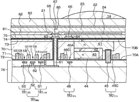
1. An imaging element, comprising:
a photoelectric conversion unit that includes:
a first electrode, a photoelectric conversion layer, and a second electrode;
a charge storage electrode that has a region, wherein the region is opposite to the first electrode via an insulating layer; and
a transfer control electrode that is opposite to the first electrode and the charge storage electrode via the insulating layer, wherein
the photoelectric conversion layer is above the charge storage electrode via the insulating layer,
the transfer control electrode includes two transfer control electrode segments,
the two transfer control electrode segments and two sides of each charge storage electrode of a plurality of charge storage electrodes are on both sides of the region,
the charge storage electrode is included in the plurality of charge storage electrodes,
the two transfer control electrode segments are adjacent to the two sides of each charge storage electrode of the plurality of charge storage electrodes,
the two sides of each charge storage electrode of the plurality of charge storage electrodes are a first side and a second side,
a length of the first side is L1,
a length of the second side is L2,
the two transfer control electrode segments include a transfer control electrode segment along the first side and a transfer control electrode segment along the second side,
a distance between the first electrode and an end of the transfer control electrode segment along the first side is in a range of 0.02×L1 to 0.5×L1, and
a distance between the first electrode and an end of the transfer control electrode segment along the second side is in a range of 0.02×L2 to 0.5×L2.
|