| CPC H04N 25/745 (2023.01) [H04N 25/46 (2023.01); H04N 25/583 (2023.01)] | 21 Claims |
|
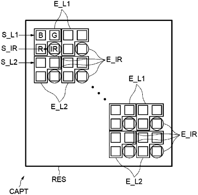
1. An image sensor comprising:
an array of photosensitive pixels dedicated to components of a spectrum of the light, each pixel including
a photosensitive semiconductor region,
a transfer gate coupled between the photosensitive region, and
a transfer node, the transfer node having a capacitive value defining a charge-to-voltage conversion factor of each pixel,
the array of photosensitive pixels being arranged according to a periodic pattern of macro-pixels each dedicated to one component, and each including a first pixel and a second pixel dedicated to this component, the capacitive value of the transfer node of the first pixel defining a first charge-to-voltage conversion factor, the capacitive value of the transfer node of the second pixel defining a second charge-to-voltage conversion factor different from the first charge-to-voltage conversion factor.
|