| CPC H04L 9/0637 (2013.01) [G06F 3/0679 (2013.01); G06F 21/602 (2013.01); G06F 21/72 (2013.01); G06F 21/76 (2013.01); H04L 9/0643 (2013.01); H04L 9/14 (2013.01); H04L 9/3239 (2013.01); H04L 67/1023 (2013.01); H04L 67/1097 (2013.01); H04L 9/50 (2022.05); H04L 67/104 (2013.01)] | 27 Claims |
|
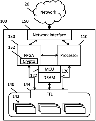
1. A solid state drive (SSD) comprising:
a non-volatile memory;
a storage controller;
a network interface; and
a processing unit configured to:
implement a blockchain algorithm; and
store data associated with a blockchain corresponding to the blockchain algorithm in the non-volatile memory via the storage controller included within the SSD; and
a processor having memory coupled thereto, the memory having instructions stored thereon that cause the processor to:
send and receive data associated with the blockchain via the network interface; and
control the processing unit to execute the blockchain algorithm on the data associated with the blockchain,
the non-volatile memory, the storage controller, the network interface, and the processing unit being integrated into a single SSD.
|