| CPC H04B 1/16 (2013.01) [H03F 3/19 (2013.01); H03F 3/245 (2013.01); H04L 27/06 (2013.01); H03F 2200/451 (2013.01)] | 20 Claims |
|
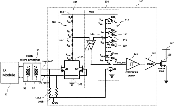
1. A first receiver circuit comprising:
a first resistor string comprising a plurality of resistors coupled in series;
a second resistor string comprising a plurality of resistors coupled in series;
a first transistor and a second transistor coupled in parallel, wherein a first load path terminal of the first transistor and a first load path terminal of the second transistor are coupled to a reference voltage node, wherein a second load path terminal of the first transistor and a second load path terminal of the second transistor are coupled to a first end of the first resistor string, with a second end of the first resistor string being coupled to a supply voltage node, wherein a first control terminal of the first transistor and a second control terminal of the second transistor are coupled to a first input terminal of the receiver circuit and a second input terminal of the receiver circuit, respectively;
a third transistor, wherein a first load path terminal of the third transistor is coupled to the reference voltage node, and a second load path terminal of the third transistor is coupled to a first end of the second resistor string, with a second end of the second resistor string being coupled to the supply voltage node, wherein a control terminal of the third transistor is coupled to a bias voltage node;
a plurality of switches coupled in parallel, wherein each switch of the plurality of switches has a first terminal and a second terminal, wherein the first terminals of the plurality of switches are coupled to a first node, wherein the second terminal of each switch is coupled to a terminal of a respective resistor in the second resistor string; and
an amplifier, wherein a first input terminal of the amplifier is coupled to the first node, and a second input terminal of the amplifier is coupled to a second node in the first resistor string.
|