| CPC H03L 7/0816 (2013.01) [H03K 5/134 (2014.07); H03L 7/0895 (2013.01); H03L 7/087 (2013.01)] | 9 Claims |
|
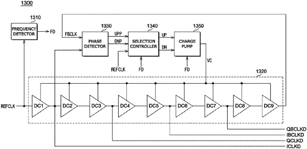
1. A delay locked loop circuit comprising:
a frequency detector configured to detect a frequency of a reference clock signal to generate a frequency detection signal;
a delay line configured to delay, based on a delay control voltage, the reference clock signal to generate an internal clock signal and a feedback clock signal;
a phase detector configured to compare phases of the internal clock signal and the feedback clock signal to generate a first detection signal and a second detection signal;
a selection controller configured to provide the first detection signal and the second detection signal respectively as an up-signal and a down-signal when the frequency detection signal is disabled, and to provide the reference clock signal as the up-signal and the down-signal when the frequency detection signal is enabled; and
a charge pump configured to generate the delay control voltage based on the up-signal and the down-signal.
|