| CPC H03K 19/17728 (2013.01) [H03K 19/1737 (2013.01); H03K 19/17758 (2020.01); H03K 19/17772 (2013.01)] | 14 Claims |
|
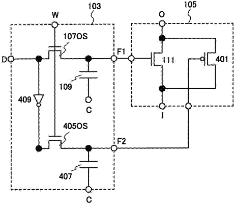
1. A semiconductor device comprising a circuit, the circuit comprising:
a first transistor;
a second transistor;
a third transistor;
a fourth transistor;
a first capacitor; and
a second capacitor,
wherein one electrode of the first capacitor is electrically connected to one electrode of the second capacitor,
wherein one of a source and a drain of the first transistor is electrically connected to one of a source and a drain of the second transistor,
wherein a gate of the first transistor is electrically connected to a gate of the second transistor,
wherein the other of the source and the drain of the first transistor is electrically connected to a gate of the third transistor,
wherein one of a source and a drain of the third transistor is electrically connected to one of a source and a drain of the fourth transistor,
wherein the first transistor comprises an oxide semiconductor in a channel formation region,
wherein the second transistor comprises an oxide semiconductor in a channel formation region, and
wherein the third transistor comprises crystalline silicon in a channel formation region.
|