| CPC H03K 5/1565 (2013.01) [G11C 7/222 (2013.01); H03K 5/134 (2014.07); H03K 5/135 (2013.01)] | 20 Claims |
|
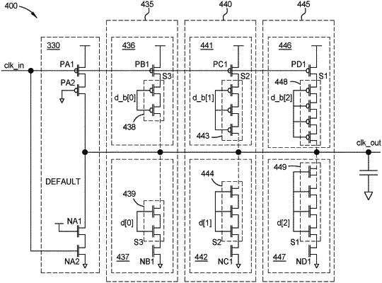
1. An integrated circuit for correcting an input clock signal, comprising:
a first leg circuit; and
a second leg circuit;
wherein the first leg circuit and the second leg circuit both comprise a charging circuit and a discharging circuit, wherein each charging circuit comprises a first plurality of transistors in series and each discharging circuit comprises a second plurality of transistors in series, wherein the charging circuit is coupled to the discharging circuit in series;
wherein a number of transistors of the first plurality of transistors in the first leg circuit is different from a number of transistors of the first plurality of transistors in the second leg circuit.
|