| CPC H03K 3/356121 (2013.01) [H03K 3/012 (2013.01); H03K 3/0375 (2013.01)] | 20 Claims |
|
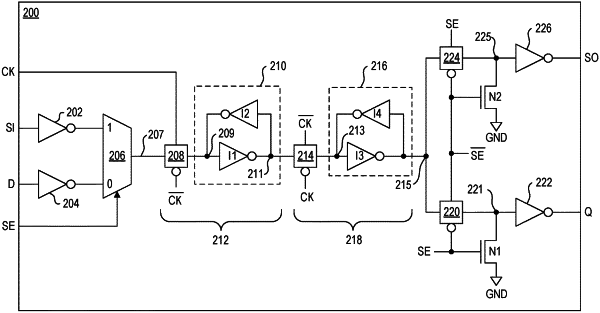
1. A flip-flop, comprising:
a scan enable input for receiving a scan enable signal;
a clock input for receiving a clock signal;
input select circuitry that is configured to select between a data input and a scan input based on a state of the scan enable signal for providing a selected input on a first node;
latching circuitry comprising a plurality of latches coupled in series between the first node and a preliminary output node that is configured to latch the selected input to the preliminary output node in response to transitions of the clock signal; and
output select circuitry that is configured to provide a state of the preliminary output node to a selected one of a scan output and a data output based on a state of the scan enable signal, and that is configured to mask the preliminary output node from the data output when the scan output is selected, wherein the output select circuitry comprises:
a first pass gate controlled by the scan enable signal having an input coupled to the preliminary output node and having an output, and a first buffer having an input coupled to the output of the first pass gate and having an output providing the data output; and
a second pass gate controlled by the scan enable signal having an input coupled to the preliminary output node and having an output, and a second buffer having an input coupled to the output of the second pass gate and having an output providing the scan output.
|