| CPC H03F 3/60 (2013.01) [H01P 3/06 (2013.01); H01P 5/10 (2013.01); H03F 3/21 (2013.01); H03H 7/38 (2013.01); H03H 7/463 (2013.01)] | 32 Claims |
|
1. An apparatus, comprising:
a plurality of power amplifiers;
a power combiner circuit, comprising:
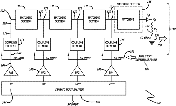
a plurality of input ports, each input port receiving an input signal from a power amplifier among the plurality of power amplifiers;
an impedance matching network topology configured between the plurality of input ports and an output port, including
a plurality of impedance matching sections between each input port and the output port, plurality of impedance matching sections including a coupling element configured between each input port and a receiving node in a plurality of cascading receiving nodes, a plurality of internodal matching sections between receiving nodes in the plurality of cascading receiving nodes, and an output matching section coupled between the output port and a last receiving node in the plurality of cascading receiving nodes,
the impedance matching network topology having a simultaneously-matched impedance condition between the input ports and the output port, achieved by a) calculating a current from each input port and seen at each receiving node, and b) calculating an impedance of each coupling element, each internodal matching section, and the output matching section for a desired bandwidth for a specific broadband frequency response, so that a load impedance at the output port is equal to an impedance seen at each input port; and
a phase shifting component configured to adjust a difference in signal phase so that the input signal seen at each receiving node has the same signal phase; and
a power electronics system coupled to the output port and configured to operate at the simultaneously-matched impedance condition for the desired bandwidth.
|