| CPC H02M 3/158 (2013.01) [H02M 1/08 (2013.01); H02M 1/0022 (2021.05); H02M 3/156 (2013.01)] | 22 Claims |
|
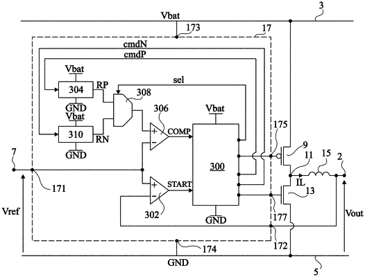
1. A voltage converter comprising:
a first transistor coupled between a first rail configured to receive a supply voltage and a first node;
a second transistor coupled between the first node and a second rail coupled to a reference voltage;
an inductance coupled between the first node and a second node configured to deliver an output voltage;
a first ramp generator configured to deliver a first voltage ramp with a slope proportional to a first voltage difference between the supply voltage and the output voltage; and
a second ramp generator configured to deliver a second voltage ramp with a slope proportional to the first voltage difference,
wherein, at each operating cycle of the voltage converter:
the first transistor is maintained in the on state for a first time period, the first time period being determined from a comparison of the first voltage ramp and the output voltage or a voltage set point, and
the second transistor is maintained in the on state for a second time period, the second time period being determined from a comparison of the second voltage ramp and the output voltage or the voltage set point.
|