| CPC H02J 7/00712 (2020.01) [H02J 2207/20 (2020.01); H04R 1/1016 (2013.01); H04R 1/1025 (2013.01)] | 6 Claims |
|
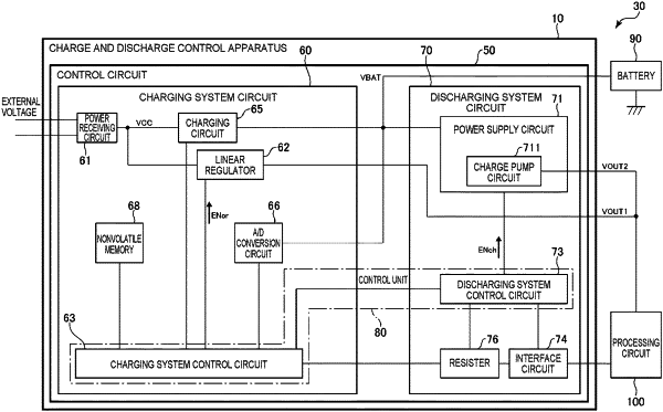
1. A charge and discharge control apparatus, comprising:
a first power supply circuit configured to supply power to a power supply target based on received power;
a charging circuit configured to charge a charging target based on received power;
a second power supply circuit configured to supply power to the power supply target based on discharge power output from the charging target, wherein the charging target is disposed between the charging circuit and the second power supply circuit; and
a control unit configured to control operations of the first power supply circuit and the second power supply circuit, wherein when a voltage of the charging target is lower than a predetermined value, the control unit causes the first power supply circuit to supply power to the power supply target,
wherein when the voltage of the charging target is the predetermined value or higher, the control unit causes the second power supply circuit to supply power to the power supply target.
|