| CPC H01S 5/02255 (2021.01) [H01S 5/0087 (2021.01); H01S 5/028 (2013.01); H01S 5/02216 (2013.01); H01S 5/02234 (2021.01); H01S 5/185 (2021.01); H01S 5/4012 (2013.01); H01S 5/4031 (2013.01); H01S 5/4075 (2013.01)] | 13 Claims |
|
1. A semiconductor laser comprising:
a carrier,
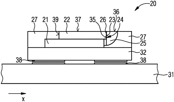
an edge-emitting laser diode which is arranged on the carrier and which has an active zone for generating laser radiation and a facet with a radiation exit area,
an optical element which covers the facet,
a connecting material which is arranged between the optical element and the facet,
a molded body which covers the laser diode and the optical element at least in places, wherein
the optical element is at least partially transparent to the laser radiation emitted by the laser diode during operation, and
the optical element is designed to change the main propagation direction of the laser radiation entering the optical element during operation,
the optical element has a radiation exit side, and
a photocatalytically acting layer is applied on the radiation exit side of the optical element to support decomposition reactions on the radiation exit side.
|