| CPC H01R 4/16 (2013.01) [H01R 12/724 (2013.01); H01R 13/639 (2013.01); H01R 13/6473 (2013.01); H01R 24/50 (2013.01)] | 5 Claims |
|
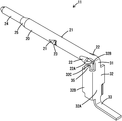
1. A connector, comprising:
an inner conductor terminal;
an outer conductor terminal for covering an outer periphery of the inner conductor terminal; and
a dielectric arranged between the inner conductor terminal and the outer conductor terminal,
wherein:
the inner conductor terminal includes a tubular terminal body extending in a front-rear direction and projections provided on the terminal body and to be locked to the dielectric,
a plurality of the projections are provided at an interval in the front-rear direction, and
a rear end of a rear projection is arranged behind a rear surface of the dielectric, the rear projection being the projection arranged at a rearmost position, out of the plurality of projections provided at an interval in the front-rear direction.
|