| CPC H01Q 1/243 (2013.01) [H01Q 1/38 (2013.01); H01Q 5/35 (2015.01); H01Q 21/28 (2013.01); H01R 12/79 (2013.01); H01R 13/6691 (2013.01); H05K 1/028 (2013.01); H05K 1/0218 (2013.01); H05K 1/0243 (2013.01); H05K 1/115 (2013.01); H05K 1/142 (2013.01); H05K 1/148 (2013.01); H05K 1/18 (2013.01); H05K 7/1427 (2013.01); H05K 2201/0999 (2013.01); H05K 2201/09609 (2013.01); H05K 2201/10098 (2013.01)] | 20 Claims |

|
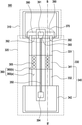
1. A portable communication device comprising:
a housing;
a first printed circuit board (PCB) disposed in the housing;
a wireless communication circuit mounted on the first PCB; and
a second PCB including:
a connection part connected with the first PCB;
a first PCB portion extended from the connection part and having greater flexibility than the connection part;
a second PCB portion extended from the first PCB portion and having less flexibility than the first PCB portion;
a third PCB portion extended from the second PCB portion and having greater flexibility than the second PCB portion;
a fourth PCB portion extended from the third PCB portion and having less flexibility than the first PCB portion;
a signal line extended to the connection part along the first, second, third, and fourth PCB portions; and
vias arranged in at least a partial area of the second PCB portion or the fourth PCB portion,
wherein a portion of the signal line is located between some of the vias.
|