US 11,749,875 B2
Chip antenna and manufacturing method thereof
Chin Mo Kim, Suwon-si (KR); Sungyong An, Suwon-si (KR); and Jae Yeong Kim, Suwon-si (KR)
Assigned to Samsung Electro-Mechanics Co., Ltd., Suwon-si (KR)
Filed by Samsung Electro-Mechanics Co., Ltd., Suwon-si (KR)
Filed on Jun. 9, 2021, as Appl. No. 17/343,235.
Claims priority of application No. 10-2021-0000885 (KR), filed on Jan. 5, 2021.
Prior Publication US 2022/0216586 A1, Jul. 7, 2022
Int. Cl. H01Q 1/00 (2006.01); H01Q 1/22 (2006.01); H05K 1/18 (2006.01); H05K 3/10 (2006.01); H01Q 9/04 (2006.01); H05K 1/11 (2006.01)
CPC H01Q 1/2283 (2013.01) [H01Q 9/0407 (2013.01); H05K 1/11 (2013.01); H05K 1/181 (2013.01); H05K 3/10 (2013.01); H05K 2201/10098 (2013.01)] 20 Claims
OG exemplary drawing
 
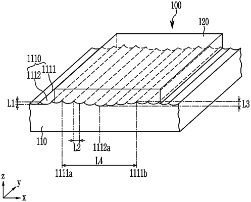
1. A chip antenna comprising:
a substrate comprising a concavo-convex pattern on a surface thereof; and
a conductor pattern disposed on the surface of the substrate comprising the concavo-convex pattern,
wherein a convex portion extending in one direction and a concave portion extending in one direction are alternately disposed in the concavo-convex pattern.