| CPC H01L 33/62 (2013.01) [H01L 33/502 (2013.01); H01L 33/56 (2013.01); H01L 33/642 (2013.01)] | 20 Claims |
|
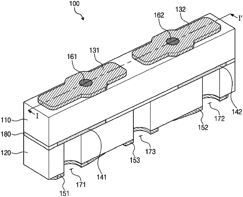
1. A light emitting device, comprising:
a substrate;
a light source disposed on an upper surface of the substrate and configured to emit light, the light source including a light emitter, a first electrode pad, and a second electrode pad;
an electrical contact disposed on the upper surface of the substrate and including a first terminal electrically connected to the substrate and the first electrode pad and a second terminal electrically connected to the substrate and the second electrode pad;
a light transmitter disposed to cover at least a part of the light emitter and having a surface through which the light source emits the light, the surface being perpendicular to the upper surface of the substrate;
a first insulator disposed on a first side of the light transmitter; and
a second insulator disposed on a second side of the light transmitter that is opposite to the first side of the light transmitter, and
wherein the first insulator and the second insulator have surfaces disposed to be flush with the surface of the light transmitter.
|