| CPC H01L 33/56 (2013.01) [H01L 33/005 (2013.01); H01L 33/38 (2013.01); H01L 33/40 (2013.01); H01L 2933/005 (2013.01); H01L 2933/0016 (2013.01)] | 12 Claims |
|
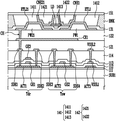
1. A display device, comprising:
a pixel circuit layer comprising a plurality of transistors;
a first partition wall and a second partition wall on the pixel circuit layer, and each protruding in a thickness direction;
a first electrode and a second electrode at a same level in the thickness direction, and on the first partition wall and the second partition wall, respectively;
a light emitting element between the first electrode and the second electrode;
a first organic pattern directly on the light emitting element; and
an insulating layer on a portion of each of the first and second electrodes,
wherein the insulating layer exposes another portion of each of the first and second electrodes.
|