| CPC H01L 33/405 (2013.01) [H01S 5/125 (2013.01); H10K 10/84 (2023.02)] | 19 Claims |
|
1. A light emitting device comprising:
a substrate;
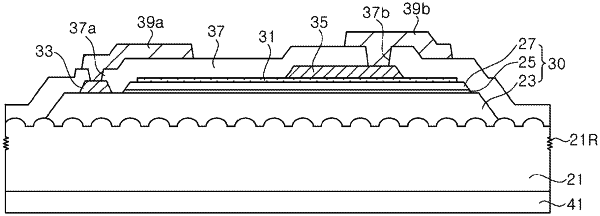
a light emitting structure disposed on one end of the substrate, the light emitting structure comprising a first conductivity type semiconductor layer and a mesa disposed on a partial region of the first conductivity type semiconductor layer;
a transparent electrode disposed on the mesa;
a contact electrode disposed on the first conductivity type semiconductor layer;
a first insulating reflection layer covering at least a portion of the light emitting structure, the transparent electrode and the contact electrode;
a first pad electrode disposed in an upper region of the transparent electrode and on the first insulating reflection layer, and electrically connected to the contact electrode;
a second pad electrode disposed in the upper region of the transparent electrode and electrically connected to the transparent electrode; and
a second insulating reflection layer disposed on an opposite end of the substrate, wherein the first insulating reflection layer, the second insulating reflection layer or both have at least two regions which have different reflectivity properties.
|